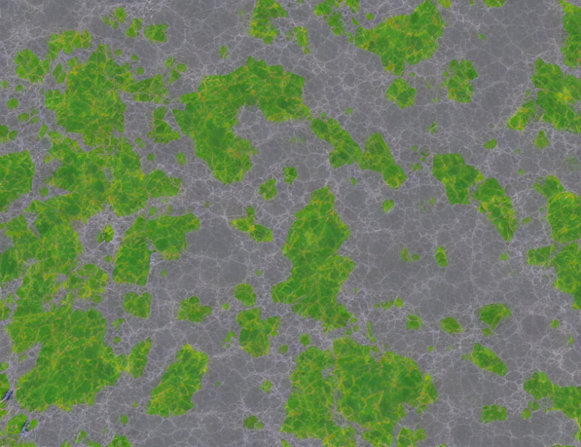
In this study, researchers used a special tool called an atomic force microscope (AFM) to observe and control the behavior of electrons and holes in a thin layer of semiconducting material called wolfram disulfide (WSe2). They found that by using highly concentrated electric fields, they could create small clusters of electrons and holes called excitonic complexes near the AFM tip. These excitonic complexes were much smaller than the distance between atoms in the material, making them incredibly useful for studying quantum phenomena at the nanoscale.
To understand how this works, think of the WSe2 layer as a big pizza with toppings of electrons and holes. The AFM tip is like a tiny fork that can pick up one of these toppings and move it around. By using the electric fields, the researchers could manipulate the location of the toppings and create clusters of them near the fork. These clusters are the excitonic complexes.
The researchers also found that the number of holes in these excitonic complexes was much larger than the number of electrons, which is unusual because normally the number of electrons is much bigger than the number of holes. This suggests that the strong electric fields used to create the excitonic complexes are causing the holes to move away from the center of the cluster and towards the edge, where they can more easily combine with other holes.
Overall, this study demonstrates a powerful new tool for controlling and observing quantum phenomena at the nanoscale. By manipulating the position and number of electrons and holes in a material using highly concentrated electric fields, researchers can create excitonic complexes that are perfect for studying quantum behavior. This could lead to new breakthroughs in fields like optoelectronics and quantum information processing.
Mesoscale and Nanoscale Physics, Physics
Exciton Dynamics in Monolayer WSe2: Local Strain Control and Valley Coherence


